MOS 6502 CPU rebuilt from 4,051 discrete transistors
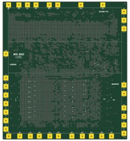
The discrete6502 is a hardware project that rebuilds the MOS 6502 CPU using 4,051 individual surface-mount transistors — no integrated chips or FPGA. The entire circuit is laid out on a custom PCB that reproduces the original silicon die's floorplan, transistor by transistor, at a scale of 291×322 mm. It is not a simulation or emulation; it runs the same dynamic NMOS logic as the original 6502, executing the same instructions at a speed of roughly 10–20 kHz.
The project solves the challenge of making a classic CPU's internal operation visible and tangible. By replacing the microscopic transistors with discrete components and placing LEDs on register bits, it allows observers to watch the processor think — seeing data flow through the datapath, decode logic, and program counter in real time.
It is designed for hardware enthusiasts, retrocomputing hobbyists, educators, and anyone interested in understanding computer architecture at the transistor level. The board includes a footprint for a Raspberry Pi Pico that serves as clock source and memory emulator, making it a self-contained teaching tool.
Preserves the original 6502's dynamic NMOS logic, where data is stored as charge on wire capacitance and must be refreshed by the clock. Not converted to modern static logic.
Uses BSS138K SOT-323 transistors for logic and LED drivers, with 1,023 pull-up resistors replacing the original's depletion-mode loads.
Every transistor is placed at the coordinates of its silicon counterpart from an actual 6502 die, scaled up from microscope photographs.
The entire board is generated via scripts from the visual6502 netlist — no hand-drawing of schematics or PCB layout at 5,421 components.
Four independent checks: switch-level simulation against original netlist, board vs. netlist comparison, copper connectivity trace, and manufacturer DRC — all must pass before fabrication.
An unpopulated footprint for a Raspberry Pi Pico 2 W provides clock generation and memory emulation, with no other equipment required to run the CPU.
55 LEDs on register bits (A, X, Y, stack pointer, program counter halves, and status flags) allow real-time observation of internal CPU state.
Yes, it executes the same instruction set as the original MOS 6502, but at a much slower speed (10–20 kHz instead of 1 MHz).
It runs at approximately 10–20 kHz, limited by the time needed to drive gates through 10 kΩ pull-up resistors. The slow speed is intentional to allow observation.
The board includes a footprint for a Raspberry Pi Pico 2 W, which serves as the clock master and memory emulator. After soldering a Pico and flashing firmware, it provides a complete system with no other equipment needed.
Yes, every transistor is placed at the die coordinates of the corresponding silicon transistor, scaled up from photographs of a real decapped 6502.
All stages — netlist transformation, component placement, routing, and verification — are performed by custom scripts. The source data comes from the visual6502 project's transistor-level netlist.
The source code and design files are available on GitHub (as mentioned in the page). The visual6502 project data used is CC BY-NC-SA.